CMOS Full Adder in 3d Studio Max

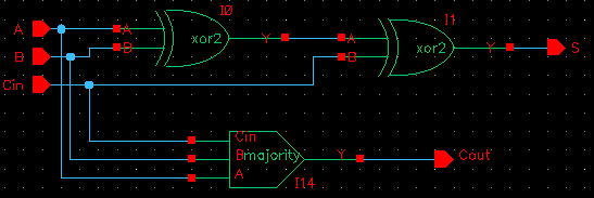
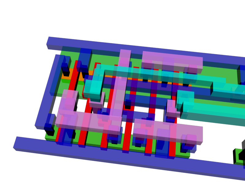
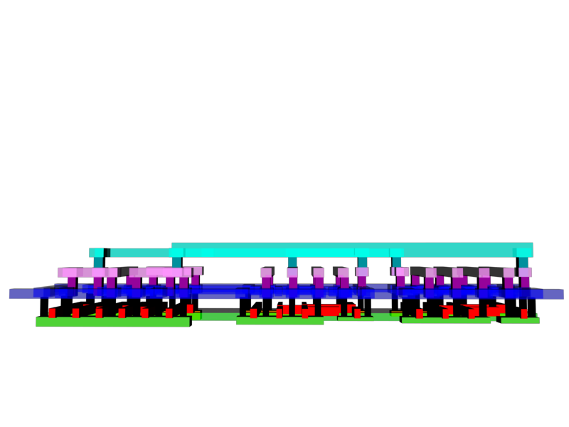
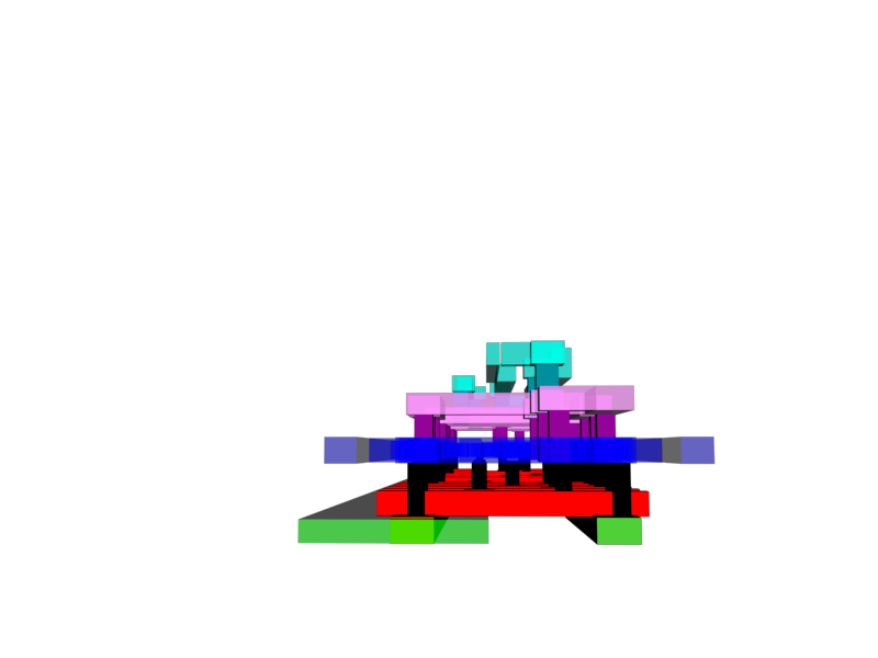
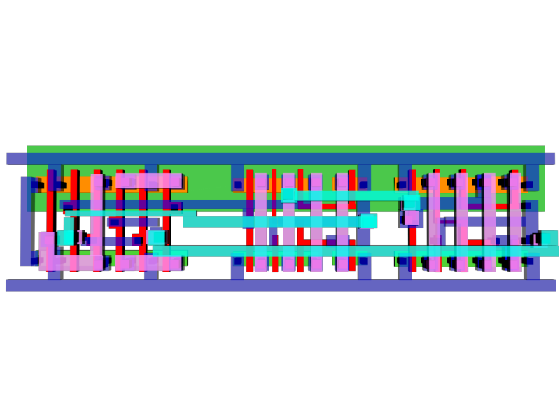
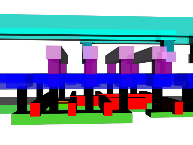
This is approximately what a CMOS Full Adder would look like in 3d. Circuit design is performed with a fixed top view, so you don't usually get to see this kind of thing. Viewing it in three dimensions lets you see the different layers actually at different heights.

fa.png
fa.png
712.00 KB
Screenshot from Cadence Layout Editor - this is how the layout for the circuit was designed.
gatelevel.png
gatelevel.png
5.83 KB
Gate-level view of the circuit. We first design the gate-level circuit to get the functionality right, and later do the actual layout.
majority1.png
majority1.png
284.89 KB
3d view of a majority gate
majority2.png
majority2.png
418.70 KB
3d view of a majority gate
majoritytransistorlevel.png
14.02 KB
Transistor-level schematic of a majority gate
nand2transistors.png
9.22 KB
Transistor-level schematic of a NAND2 gate
perspective1.png
perspective1.png
286.04 KB
3d perspective view of the full adder
perspective2.png
perspective2.png
357.58 KB
3d perspective view of the full adder
perspective3.png
perspective3.png
329.54 KB
3d perspective view of the full adder
side1.png
side1.png
121.59 KB
3d side view of the full adder
side2.png
side2.png
74.65 KB
3d side view of the full adder
top.png
top.png
213.15 KB
3d top view of the full adder
xor1.png
xor1.png
327.45 KB
3d top view of an XOR gate
xor2.png
xor2.png
620.67 KB
3d perspective view of an XOR gate
xor3.png
xor3.png
175.96 KB
3d side view of an XOR gate

Created by IrfanView